Monochrome SSD1306 128x32 OLED display
published: 7 November 2020 / updated 10 November 2020

Characteristics
For a number of applications with microcontroller boards like the Arduino the addition of a small display can be handy to show information, for instance that collected by a sensor. We discuss here how to wire a very popular monochrome 128×32 pixel graphic OLED display to an Arduino. The display uses the SSD1306 chip.
Communication runs via an I2C interface such that next to power and GND only two pins are required.
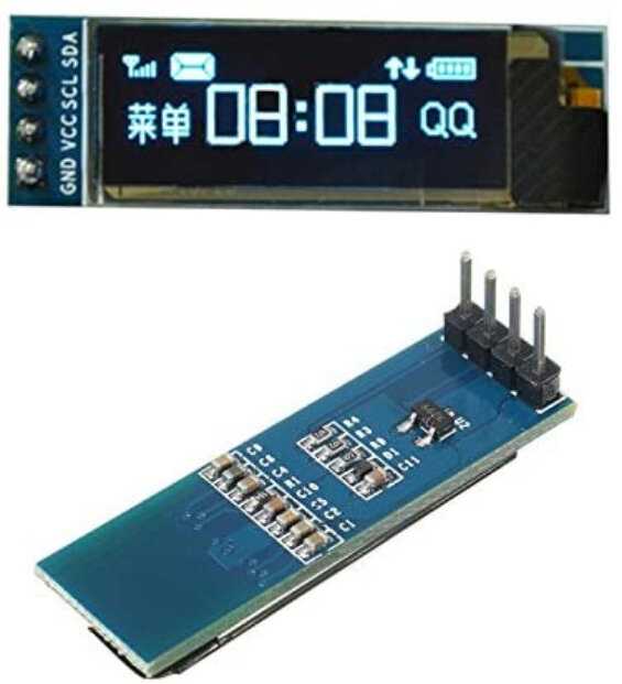
Features:
- Controller: SSD1306
- Interface: I2C
- Resolution: 128*32
- Display Size: 0.91inch
- Display Color: White
- Operating Voltage: 2.2V/5V
Device detection on the i2c bus
The SSD1306 128x32 OLED display must be electrically connected to the ARDUINO card via the i2c bus on the card.
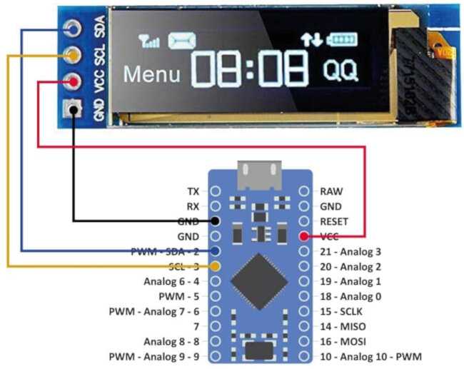
Most OLED displays, including this one, accepts both 3.3V and 5V DC power. While the Arduino Uno and Nano are typical 5V devices, newer designs such as the Internet of Things (IOT) family of ESP8266 based microcontroller boards use 3.3V logics. The 128×32 OLED display works equally well with these IOT microboards. Actually, all OLED displays run on 3.3V and power to the board as well as input signals are converted to 3.3V by an on-board voltage converter This means that the OLED display can be connected with the microcontroller board without the need of soldering resistors in series.
The program for detecting peripherals connected to the i2c bus is launched and displays:
    i2c.detect
     00 01 02 03 04 05 06 07 08 09 0a 0b 0c 0d 0e 0f
00 :                      -- -- -- -- -- -- -- -- --
10 : -- -- -- -- -- -- -- -- -- -- -- -- -- -- -- --
20 : -- -- -- -- -- -- -- -- -- -- -- -- -- -- -- --
30 : -- -- -- -- -- -- -- -- -- -- -- -- 3c -- -- --
40 : -- -- -- -- -- -- -- -- -- -- -- -- -- -- -- --
50 : -- -- -- -- -- -- -- -- -- -- -- -- -- -- -- --
60 : -- -- -- -- -- -- -- -- -- -- -- -- -- -- -- --
70 : -- -- -- -- -- -- -- --
Here, the value 3c is the address of the connected SSD1306 128x32 OLED display to the i2c bus from our ARDUINO card.
Communication I2C
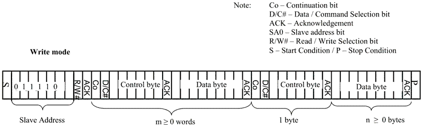
When working, ARDUINO will first send a byte that the first 7bits are address of slave device and 1 bit write/read bit, and wait for response.
After received response from slave device, ARDUINO will send a control byte, this byte defined the data following is command or data.
Slave response again, if sending command, ARDUINO will send the command which is one byte. If sending data, ARDUINO will sending data.
The control byte
It is transmitted immediately after the address of the device. It has the following structure:

A control byte mainly consists of Co and D/C# bits following by six “0” ‘s.
- If the Co bit is set as logic “0”, the transmission of the following information will contain data bytes only.
- The D/C# bit determines the next data byte is acted as a command or a data. If the D/C# bit is set to logic “0”, it defines the following data byte as a command. If the D/C# bit is set to logic “1”, it defines the following data byte as a data which will be stored at the GDDRAM. The GDDRAM column address pointer will be increased by one automatically after each data write.
Co is a continuation bit. If set to 1, the controller expects another control byte in this I2C write cycle. If set to 0, the controller will not expect to receive another control byte in this I2C write cycle
- $00: Co = 0, D/C = 0: Next byte(s) are command (non-graphics) data, after which I2C stop condition is expected
- $80: Co = 1, D/C = 0: Next byte(s) are command (non-graphics) data, after which another control byte is expected
- $40: Co = 0, D/C = 1: Next byte(s) are graphs data, after which I2C stop condition is expected
- Co = 1, D/C = 1: Is illegal combination.
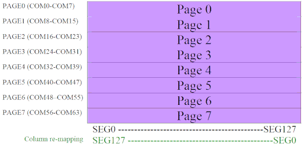
Graphic Display Data RAM (GDDRAM)
Commands
Source codes
- To use the commands on the i2c bus, you must compile the contents of the file i2c-new.txt
available here:
I2C interface management for FlashForth - To transmit commands and data to the SSD103 128x32 OLED display, you can
then compile the contents of the SSD1306oled128x32.txt file available here:
Manage monochrome OLED display SSD1306 128x32
Set Lower Column Start Address for Page Addressing Mode (00h~0Fh)
This command specifies the lower nibble of the 8-bit column start address for the display data RAM under Page Addressing Mode. The column address will be incremented by each data access.
Set Higher Column Start Address for Page Addressing Mode (10h~1Fh)
This command specifies the higher nibble of the 8-bit column start address for the display data RAM under Page Addressing Mode. The column address will be incremented by each data access.
Set Memory Addressing Mode (20h)
There are 3 different memory addressing mode in SSD1306: page addressing mode, horizontal addressing mode and vertical addressing mode. This command sets the way of memory addressing into one of the above three modes. In there, “COL” means the graphic display data RAM column.
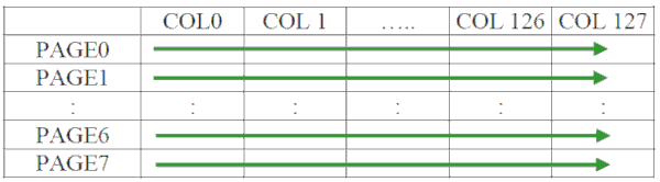
Page addressing mode (A[1:0]=10xb)
In page addressing mode, after the display RAM is read/written, the column address pointer is increased automatically by 1. If the column address pointer reaches column end address, the column address pointer is reset to column start address and page address pointer is not changed. Users have to set the new page and column addresses in order to access the next page RAM content. The sequence of movement of the PAGE and column address point for page addressing mode is shown in Figure:
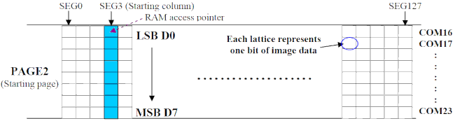
In normal display data RAM read or write and page addressing mode, the following steps are required to define the starting RAM access pointer location:
- Set the page start address of the target display location by command B0h to B7h.
- Set the lower start column address of pointer by command 00h~0Fh
- Set the upper start column address of pointer by command 10h~1Fh
For example, if the page address is set to B2h, lower column address is 03h and upper column address is 10h, then that means the starting column is SEG3 of PAGE2. The RAM access pointer is located as shown in Figure. The input data byte will be written into RAM position of column 3.
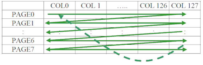
Horizontal addressing mode (A[1:0]=00b)
In horizontal addressing mode, after the display RAM is read/written, the column address pointer is increased automatically by 1. If the column address pointer reaches column end address, the column address pointer is reset to column start address and page address pointer is increased by 1. The sequence of movement of the page and column address point for horizontal addressing mode is shown in Figure. When both column and page address pointers reach the end address, the pointers are reset to column start address and page start address (Dotted line in Figure)
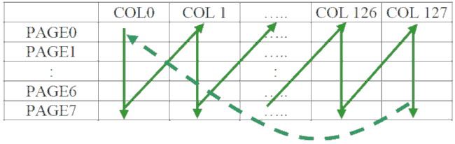
Vertical addressing mode: (A[1:0]=01b)
In vertical addressing mode, after the display RAM is read/written, the page address pointer is increased automatically by 1. If the page address pointer reaches the page end address, the page address pointer is reset to page start address and column address pointer is increased by 1. The sequence of movement of the page and column address point for vertical addressing mode is shown in Figure. When both column and page address pointers reach the end address, the pointers are reset to column start address and page start address (Dotted line in Figure)
In normal display data RAM read or write and horizontal / vertical addressing mode, the following steps are required to define the RAM access pointer location:
- Set the column start and end address of the target display location by command 21h.
- Set the page start and end address of the target display location by command 22h.
Example is shown in Figure.
Set Column Address (21h)
This triple byte command specifies column start address and end address of the display data RAM. This command also sets the column address pointer to column start address. This pointer is used to define the current read/write column address in graphic display data RAM. If horizontal address increment mode is enabled by command 20h, after finishing read/write one column data, it is incremented automatically to the next column address. Whenever the column address pointer finishes accessing the end column address, it is reset back to start column address and the row address is incremented to the next row.
Set Page Address (22h)
This triple byte command specifies page start address and end address of the display data RAM. This command also sets the page address pointer to page start address. This pointer is used to define the current read/write page address in graphic display data RAM. If vertical address increment mode is enabled by command 20h, after finishing read/write one page data, it is incremented automatically to the next page address. Whenever the page address pointer finishes accessing the end page address, it is reset back to start page address.
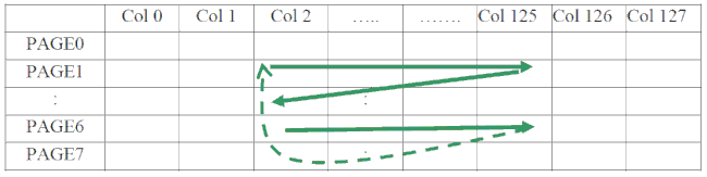
The figure below shows the way of column and page address pointer movement through the example: column start address is set to 2 and column end address is set to 125, page start address is set to 1 and page end address is set to 6; Horizontal address increment mode is enabled by command 20h. In this case, the graphic display data RAM column accessible range is from column 2 to column 125 and from page 1 to page 6 only. In addition, the column address pointer is set to 2 and page address pointer is set to 1. After finishing read/write one pixel of data, the column address is increased automatically by 1 to access the next RAM location for next read/write operation (solid line in Figure). Whenever the column address pointer finishes accessing the end column 125, it is reset back to column 2 and page address is automatically increased by 1 (solid line in Figure). While the end page 6 and end column 125 RAM location is accessed, the page address is reset back to 1 and the column address is reset back to 2 (dotted line in Figure).
Set Display Start Line (40h~7Fh)
This command sets the Display Start Line register to determine starting address of display RAM, by selecting a value from 0 to 63. With value equal to 0, RAM row 0 is mapped to COM0. With value equal to 1, RAM row 1 is mapped to COM0 and so on.
Refer to Table 10-1 for more illustrations.
Set Contrast Control for BANK0 (81h)
This command sets the Contrast Setting of the display. The chip has 256 contrast steps from 00h to FFh. The segment output current increases as the contrast step value increases.
flash
\ set contrast
stream: contrast.max ( -- )
    $81 c,  \ SETCONTRAST
    $fa c,  \ value between 00..fe
    ;stream
ram
Set Segment Re-map (A0h/A1h)
This command changes the mapping between the display data column address and the segment driver. It allows flexibility in OLED module design. Please refer to Table 9-1.
This command only affects subsequent data input. Data already stored in GDDRAM will have no changes.
Entire Display ON (A4h/A5h)
A4h command enable display outputs according to the GDDRAM contents. If A5h command is issued, then by using A4h command, the display will resume to the GDDRAM contents. In other words, A4h command resumes the display from entire display “ON” stage. A5h command forces the entire display to be “ON”, regardless of the contents of the display data RAM.
Set Normal/Inverse Display (A6h/A7h)
This command sets the display to be either normal or inverse. In normal display a RAM data of 1 indicates an “ON” pixel while in inverse display a RAM data of 0 indicates an “ON” pixel.
stream: disp.invert
    $a7 c,  \ INVERTDISPLAY
    ;stream

stream: disp.normal
    $a6 c, \ NORMALDISPLAY
    ;stream
Set Display ON/OFF (AEh/AFh)
These single byte commands are used to turn the OLED panel display ON or OFF. When the display is ON, the selected circuits by Set Master Configuration command will be turned ON. When the display is OFF, those circuits will be turned OFF and the segment and common output are in VSS state and high impedance state, respectively. These commands set the display to one of the two states:
- AEh : Display OFF
- AFh : Display ON

flash
stream: disp.on
    $af c, \ DISPLAYON
    ;stream

stream: disp.off
    $ae c, \ DISPLAYOFF
    ;stream
ram
Set Page Start Address for Page Addressing Mode (B0h~B7h)
This command positions the page start address from 0 to 7 in GDDRAM under Page Addressing Mode.
Horizontal Scroll Setup (26h/27h)
This command consists of consecutive bytes to set up the horizontal scroll parameters and determines the scrolling start page, end page and scrolling speed.
Before issuing this command the horizontal scroll must be deactivated (2Eh). Otherwise, RAM content may be corrupted.
The SSD1306 horizontal scroll is designed for 128 columns scrolling.
Ce code transmet lers l'afficheur OLED SSD1306 128x32 une trame qui déclenche le glissement latéral vers la droite:
flash
stream: scroll.RIGHT
    $27 c, \ $27 constant LEFT
    $00 c,  \ dummy byte
    $00 c,  \ start page
    $00 c,  \ time interval
    $07 c,  \ end page
    $00 c,  \ dummy byte
    $ff c,  \ dummy byte
    $2f c,  \ SCROLLON
    ;stream
ram
Deactivate Scroll (2Eh)
This command stops the motion of scrolling. After sending 2Eh command to deactivate the scrolling action, the ram data needs to be rewritten.
flash
\ Stop scroll
stream: scroll.off ( -- )
    $2e c,  \ SCROLLOFF
    ;stream
ram